We interviewed former Professor Iga with the following 5 questions ( as Part 1 ):
This interview took place on April 16th, 2026.
We would like to begin by asking about your research.
In the last issue of this interview, Professor Hiroshi Amano appeared, who is very well-known as one of Nobel laureates on Blue LED. So, I feel that I had better explain a bit of my career as a researcher on semiconductor lasers, particularly on vertical-cavity surface-emitting laser known as VCSEL. Before addressing your main questions, I think I should start with what might be called “Question 0”: Who is Kenichi Iga, and what is a VCSEL? (laughs).
Q0: First, could you tell us who Kenichi Iga is, and what a VCSEL (Vertical Cavity Surface Emitting Laser) is? You are called the father of VCSEL, aren't you?
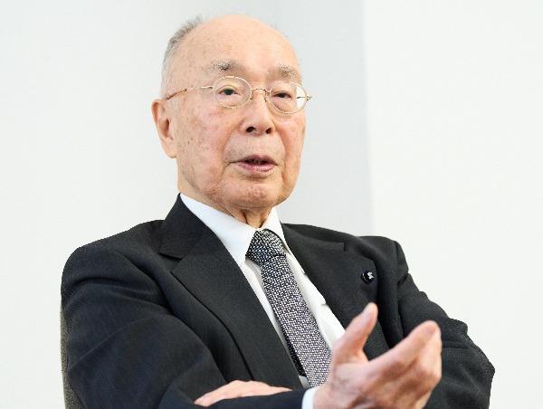
In 1977, I got the adea of what is now known as the VCSEL, ahead of anyone else realized as a working device. In October 2025, the achievement of his team was recognized as “IEEE Milestone” by the Institute of Electrical and Electronics Engineers (IEEE), an academic society with 430,000–450,000 members worldwide.
The IEEE Milestone program serves as a kind of historical archive. It recognizes technologies approximately 25 years after their invention, evaluating how much they have contributed to society. Institute of Science Tokyo which I have been belonging to had applied for this recognition several years ago, and it was officially approved of last year (in 2025). This means that our achievement has been globally acknowledged as the active starter of VCSEL.
The application was sent through the university, so the commemorative plaque honors the institution. However, the initiative research itself was my work, made possible through the contributions of members of my laboratory who collaborated with me.
So, what exactly did I conceive? Quite simply, a new type of laser.
A laser is characterized by its ability to emit light in a straight beam—like a laser pointer. By contrast, LEDs, which Professor Amano studied, emit light in all directions, which is why they are used in displays, lighting, and decorative illumination. Laser light can be tightly focused using a lens while LED light cannot: it simply forms an image of itself. In LEDs, electrons and holes recombine to produce light, much like a firework. In lasers, this light is placed inside a cavity formed by mirrors, where it is amplified through resonance and appears as coherent light. Lasers vary greatly in scale, from extremely large systems used in nuclear fusion experiments to tiny semiconductor lasers. A VCSEL is one of the smallest: it emits light perpendicular to the substrate through an aperture of only 1–10 micrometers. While the surrounding structure may be about 300 μm × 300 μm, it is still among the smallest lasers that exist.
Since the conception of this device in 1977, I have continued my research, and it has gradually found applications in many areas.
For example:
• Since 2001: computer mice and high-speed laser printers
• Local area networks (LANs) for internet communication
• Optical fiber systems connecting campuses and buildings
• Since 2017: incorporated into the iPhone X for 3D facial recognition
• Since 2020: widely used in huge data centers
In data centers, racks of computers are interconnected by optical fiber cables. Approximately 90% of the transceivers used for these connections employ VCSELs. With the rise of AI and large-scale data centers after 2024, production of these lasers has increased dramatically. Although they are small devices, their applications have expanded significantly—often in ways people are not even aware of.
My research has focused on both the fundamental principles and the underlying technologies needed to realize these devices. From the beginning, I believed they should be manufactured like silicon integrated circuits—mass-produced on wafers. Today, that is exactly how they are made. At first, however, the reception was not positive. Even when I presented my work at conferences or gave talks abroad, people said, “That will never work.” But in 1988, at the former Precision and Intelligence Laboratory, we succeeded in achieving continuous operation at room temperature. This breakthrough, proven experimentally by my successor, Professor Fumio Koyama, marked a turning point. After that, I traveled to the United States and Europe to find collaborators. Gradually its reliability improved through industrial development, and commercialization began around 2001.
In that sense, my role was to serve as a pioneer guiding the way.
Q1: What inspired you to begin your research?
I entered the former Tokyo Institute of Technology in 1959.
The first laser—the ruby laser—was created in 1960 by Theodore Maiman in the United States. As an undergraduate when I was in my first year, the laser did not exist yet. By my fourth year in 1962, I joined the laboratory of Professor Yasuharu Suematsu and began to pursue laser research for optical communication that had not existed at that time we began by building a ruby laser ourselves—from scratch. We designed the power supply, arranged polishing with a jeweler, and commissioned mirror coatings from a nearby company. After assembling everything, our ruby laser finally emitted light.
The moment a laser emits light is deeply moving. The intensity does not simply increase gradually—it suddenly jumps. This is a “phase change,” where order appears from randomness. That phenomenon is what makes lasers so fascinating. That experience inspired me to continue my research in graduate school.
Ruby lasers later found practical applications, such as rangefinders and medical treatments. I nearly suffered retinal detachment when I was a first-grade undergraduate student—before laser surgery was available. Later, lasers made such procedures far less invasive, which really illustrates the impact of the technology.
When I entered the doctoral program in 1965, Professor Suematsu recommended that I shift to a different topic since ruby lasers were already becoming practical. Following his guidance, I began working on optical communication. After completing my degree, I joined the Precision and Intelligence Laboratory as a research associate, where my assigned project was the development of an atomic clock using rubidium. This clock later found practical applications, for example, in ensuring stable multi-camera switching in television broadcasting during the 1972 Sapporo Olympics.
Q2: Your work laid the foundation for optoelectronics. Were you able to foresee this impact at the time?
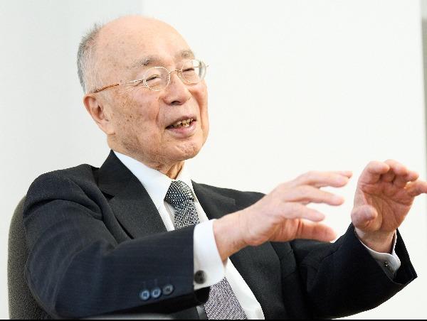
The answer is both yes and no. If everything could be predicted, research would not be interesting (laughs).
However, there was a clear sense of direction. Around 1970, both optical fibers and semiconductor lasers were becoming practical technologies for communication.
I aimed to create a laser that satisfied three conditions:
1. Single-mode operation
2. Monolithic fabrication on a wafer
3. Reproducibility of wavelength.
After much effort without success, I explored other approaches. Then, one night, I suddenly had an idea: instead of shortening the cavity horizontally, why not make it vertical?
By placing mirrors above and below an active layer, the concept of the VCSEL appeared. That was March 22, 1977. We quickly began experiments, and by 1979 we achieved lasing at liquid nitrogen temperatures. It was fragile and short-lived, but it was a start. That first paper has since become the most cited in the field.
I would like to answer your question. "Yes" means that optical communication by using VCSEL was in my visible target and realized as Local Area Networks. "No" means that computer mice, 3D face recognition, and even atomic clocks are my surprise.
Q3: In 1979, your idea was considered impractical. How did you feel at the time?
Many people told me it would never work unless it could run continuously at room temperature.
Even at Bell Labs where I stayed as guest in 1979, most researchers dismissed it. However, a few people encouraged me—including my mentor Professor Suematsu. In fact, I often say that at the time, there were only three people in the world who supported the idea: Prof. Suematsu, Dr. Mike Duguay, and Dr. Yuriy Popov.
After returning to Japan in 1980, we achieved a breakthrough by creating an extremely thin structure using etching techniques. Although it only worked at low temperatures, it proved the fundamental properties of the VCSEL in 1982.
We then worked on improving crystal growth techniques and fabrication processes introducing MOCVD. After years of effort, we finally achieved continuous operation at room temperature by Fumio Koyama in my team on September 16, 1988.
Q4: What made room-temperature continuous operation possible?
The principal factor was the improvement in crystal growth technology, particularly MOCVD.
High-quality, flat crystal layers were essential. Secondly, advances in multilayer mirror fabrication enabled high-performance reflectors. Finally, we addressed practical challenges such as heat dissipation and device packaging. When we presented this result in 1988, the reaction was dramatic. People began to reconsider VCSELs as a serious technology. From that point on and together with due to the report on micro-post laser by Jack Jewell of Bell Labs in 1989 interests of research and development sectors grew rapidly, ultimately leading to widespread research and practical applications.
For products related to this interview, please check this page.
Products & Materials
Kenichi Iga
Kenichi Iga received his B.E. in Electrical Engineering from the Tokyo Institute of Technology in 1963 and his Ph.D. in Engineering from the same institution in 1968. He served as President of the Tokyo Institute of Technology from 2007 to 2012. He has also held prominent leadership roles, including President of the Institute of Electronics, Information and Communication Engineers (IEICE) and Executive Director of the Japan Society for the Promotion of Science (JSPS).
Professor Iga is known as the inventor of the Vertical Cavity Surface Emitting Laser (VCSEL), which is widely used as a light source in high-speed data communications. His work has laid the foundation for optical interconnect technologies on the Internet and data centers, as well as for the broader field of optoelectronics. He was awarded the IEEE Edison Medal in 2021, named a Person of Cultural Merit (Japan) in 2022, and recognized with an IEEE Milestone in 2025.